Direct FIB with high resolution or 3-dimensional structures
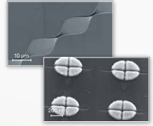
1-mm fluidic channel and array of plasmonic gold cakes
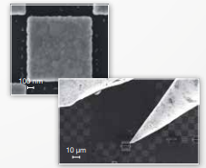
Expanded capabilities due to SEM high resolution inspection, gas inspection and nano manipulation
Excellence in FIB Nanofabrication
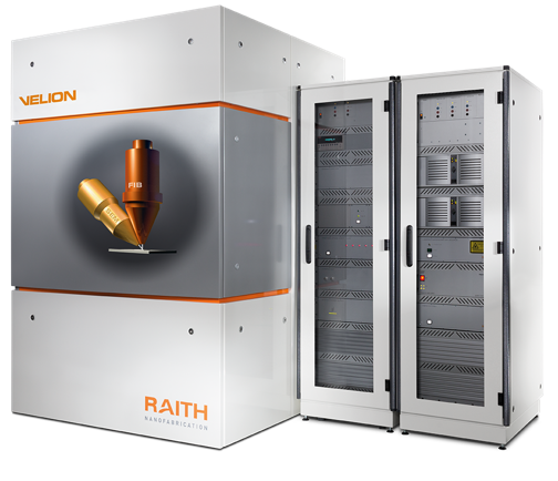
VELION challenges the nanofabrication by realizing the synergy of a focused ion beam and lithography platform. Direct FIB processing techniques are complemented by the highest-accuracy laser interferometer stage.
By choosing and optimizing versatile techniques, it helps to apply direct and simplified process with repeated accurate results over extended time and area.
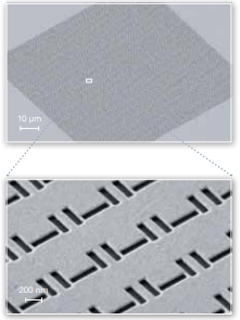
stable and automated FIB milling enables large arrays of high-resolution features, as required for plasmonic applications
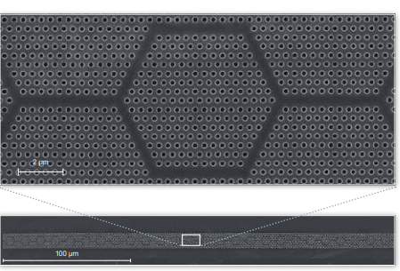
Write field stitching allows for direct milling of long wave guides with offsets on 10 nm scale only
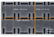
Detailed in-situ SEM inspection of plasmonic features created by FIB milling
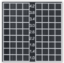
EBL test pattern for determining the line width for different dose factors
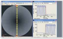
The roundness of an X-ray lens is checked by advanced SEM metrology line scans
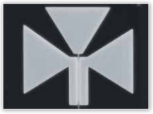
Demo example (transistor like pattern) showing EBL overlay capabilities
SEM capabilities for inspection and lithography
SEM high-resolution imaging and automated metrology can be applied to various patterning results and microscopy samples.
Electron Beam Lithography with the optics design and powerful patterning engine for the SEM column, the system offers EBL workhorse capabilities. This enables sophisticated applications in nano electronics, physics, and photonics, and combines with FIB nanofabrication in one instrument. VELION offers the unique opportunity of complementary advanced lithography with both ion and electron beams in a single dedicated nanofabrication system.
Benefits of SEM column support for FIB processes
The field emission SEM column significantly expands the capabilities of VELION. VELION helps to provide all the required capabilities of a FIB tool for TEM, APT or other sample preparation.
The X-section analysis is employed for high resolution imaging of FIB X-sectional cuts.
The process checks helps in the inspection of all features created by the ion beam. Given the direct patterning techniques of FIB, it is possible to check results and optimize parameters in an in-situ closed-loop approach for very efficient process development
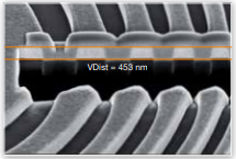
X-sectional process control of an X-ray Fresnel zone plate fabricated in 500nm thick gold
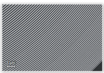
Top-down high resolution SEM imaging used for lateral process control of FIB milling
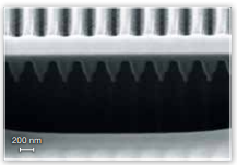
The 3-dimensional shape of a special antireflective grating is revealed by X-section analysis
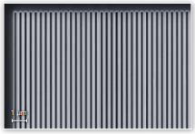
Placement, straightness and pitch of the 3-dimensional grating are checked by SEM inspection
FIB nanofabrication
- Versatile and accurate sub-10-nm FIB nanofabrication
- Excellent beam spot characteristics and lowest beam tails (nanoFIB Three
- Nanofabrication with multiple ion species beyond gallium (IONselect technology)
- Direct patterning using ion milling for fastest time to results
- Resist exposure, maskless ion implantation, and hardmasking
- Laser Interferometer Stage enables write field stitching and continuous writing

FIB Preparation
- Ion-beam-induced deposition and gas-assisted etching
- X-sectioning at multiple sites for correlated inspection
- Site specific low damage preparation with accurate end-point control
- Nanomanipulators for in-situ lift-out, probing and profilometry
- Resist exposure, maskless ion implantation, and hardmasking
- TEM lamella, APT tips or other sample preparation
SEM Inspection
- High resolution imaging and automated metrology
- Test arrays and repeated processes with in-situ correlated workflow
- In depth control of 3-dimensional FIB processes
- Advanced stage setup for large area sample inspection with CAD navigation

SEM Lithography
- Column design with electromagnetic focusing and electrostatic deflection
- High lithography resolution and fast deflection in calibrated write fields
- Full software package with GDSII handling and various patterning strategies
- EBL capabilities for sophisticated applications in nano technology research
