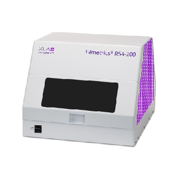
- Tool Configurations: 4 Point-Probe (4PP) Dual Configuration / Eddy Current (EC)
- Metal film and backside layer thickness measurements
- Substrate resistivity
- Sheet resistance
- Thin film thickness or resistivity
- Sheet and bulk conductivity
3D Profilometer: Profilm3D
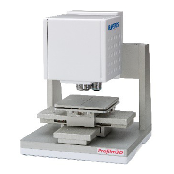
- Scanning range: 0nm – 10mm
- PSI & WLI measurement modes
- Color imaging option
- Intuitive GUI
- Step-height repeatability 0.1%
- ISO 25178 compliant (roughness)
- Best value-for-price in the market
F50 Film Thickness Measurement
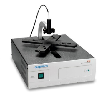
- Fast (within a 1 sec or less)
- Non-contact
- Accurate: 1nm or 0.2%
- No preprocessing required (no step height needed)
- Non-destructive
- Spot size scalable (6mm – 1µm)
Single Spot Measurements
- Measures film thickness and refractive index with a single mouse-click.
- Measures thicknesses from 1nm to 13mm, multi-layer possible
- Different probes for various surfaces
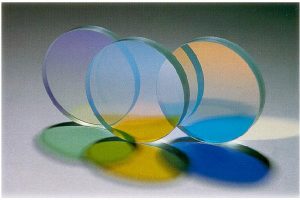
Spectral Reflectance, Refractive Index
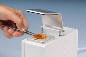
Small Coupon
Solar Photovoltaics
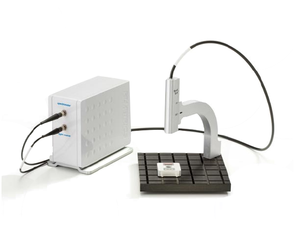
Application Examples
Biomedical Devices
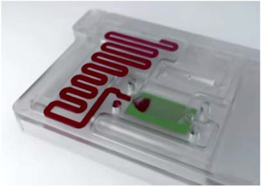
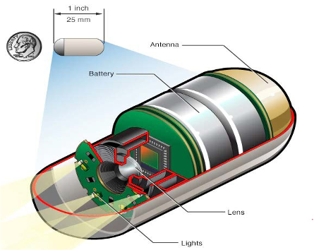
Medical Devices
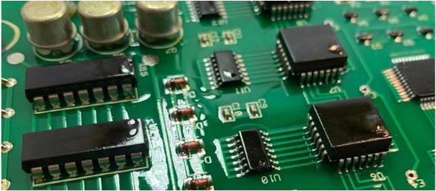
Conformal Coatings on PCB
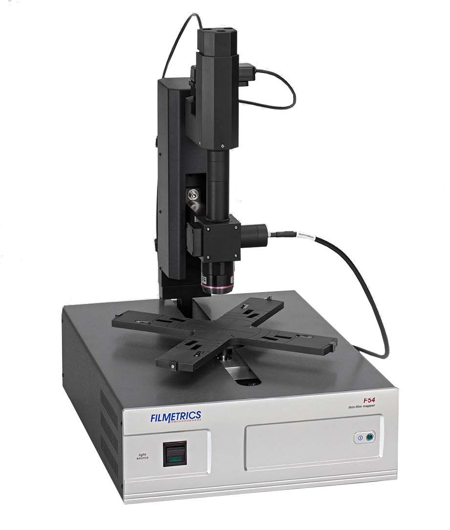
Automated Mapping
- Fully-automatic mapping of thickness and index for nearly any sample shape.
- Manual-load and robotic-load systems are available.
- SECS-GEM capable
- Automatic baseline, auto notch alignment
- Average Reflectance Mapping
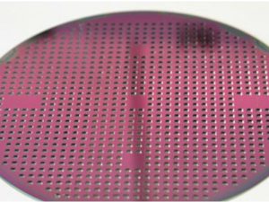
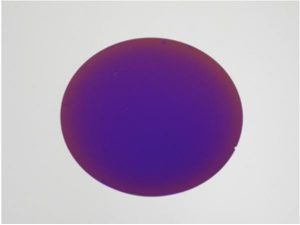
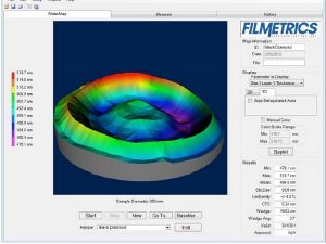
Mapping – spatial distribution
- Typical Applications
- Semiconductor films (SiO2, SiN, Poly-Si, a- Si, Photoresist, Polyimides)
- Medical devices
- Failure Analysis
- Measure / Map / Monitor remaining Si thickness on Ics
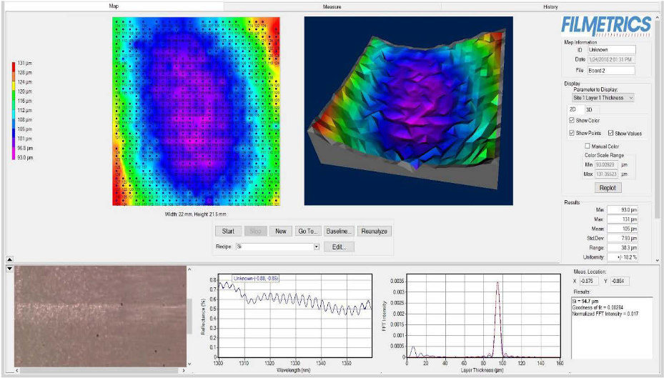
In-line Monitoring
- Measure film thickness in-line and in real-time e.g. moving films at up to seven locations with the F37.
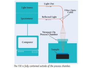
- Measure deposition rates, film thickness, optical constants (n and k), and uniformity of semiconductors and dielectric layers in real-time with the F30 spectral reflectance system.
- Sample rates as high as 100 Hz are possible at multiple measurement locations.
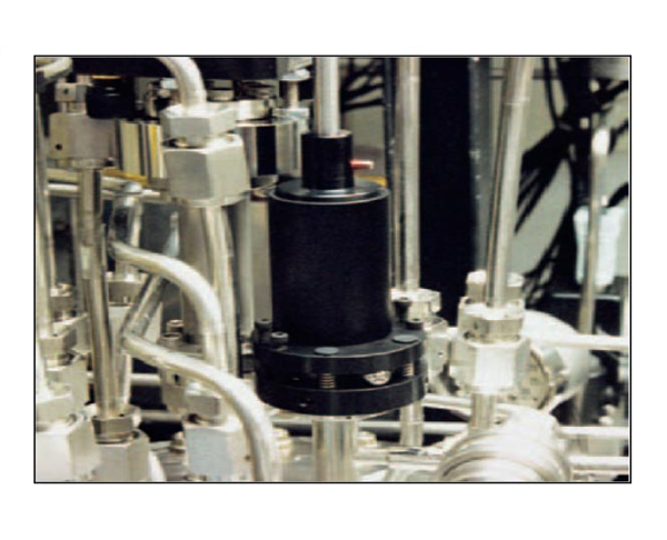
In-line Monitoring Examples
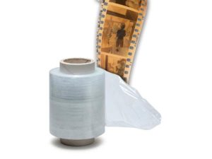
Plastic films
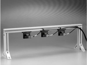
3 spot frame probe for inline measurements
R50/ R54 Applications
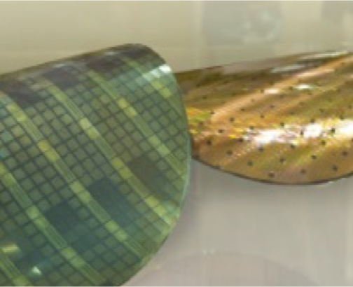
Rigid or flexible surfaces
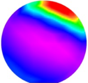
Mapping Aluminum on Silicon
Semiconductor Manufacturing
- Metal film deposition mapping
- Ion implant process mapping
- Sputter process mapping
- Bulk Si dopant mapping
R&D/Academia/Industry
- Sheet Resistance / Resistivity / Film Thickness
- Coated optical components
- Wearable technology/flexible conductive materials
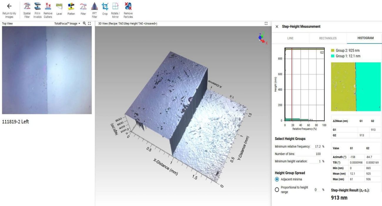
ProfilmOnline
Online surface metrology software
- Cloud-based platform to view, analyze and share 3D surface data
- Web browser- & apps-based (Android & iOS)
- Support of various file types (Filmetrics, Keyence, Bruker, etc.)
- Analyze step height, roughness, particles, dimensions
- Join (for free) our 3D optical community and share your results with your colleagues: ProfilmOnline
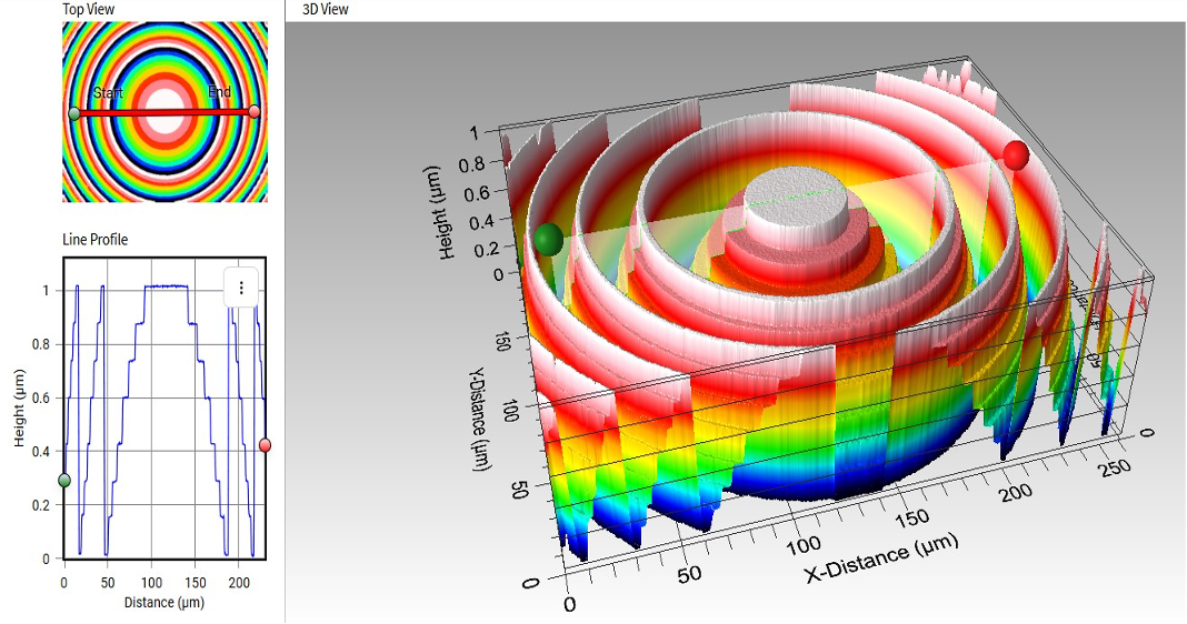
Step height
Metal Depositions
- Metal thickness
- CVD, MOCVD, PVD, etc.
