Hakuto is the leading provider of ion beam etching system from small scale system
for R&D to mass production with over 50 years of experience.

Hakuto is the leading provider of ion beam etching system from small scale system
for R&D to mass production with over 50 years of experience.
Ion Beam Etching (Milling) System
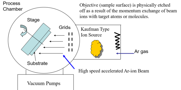
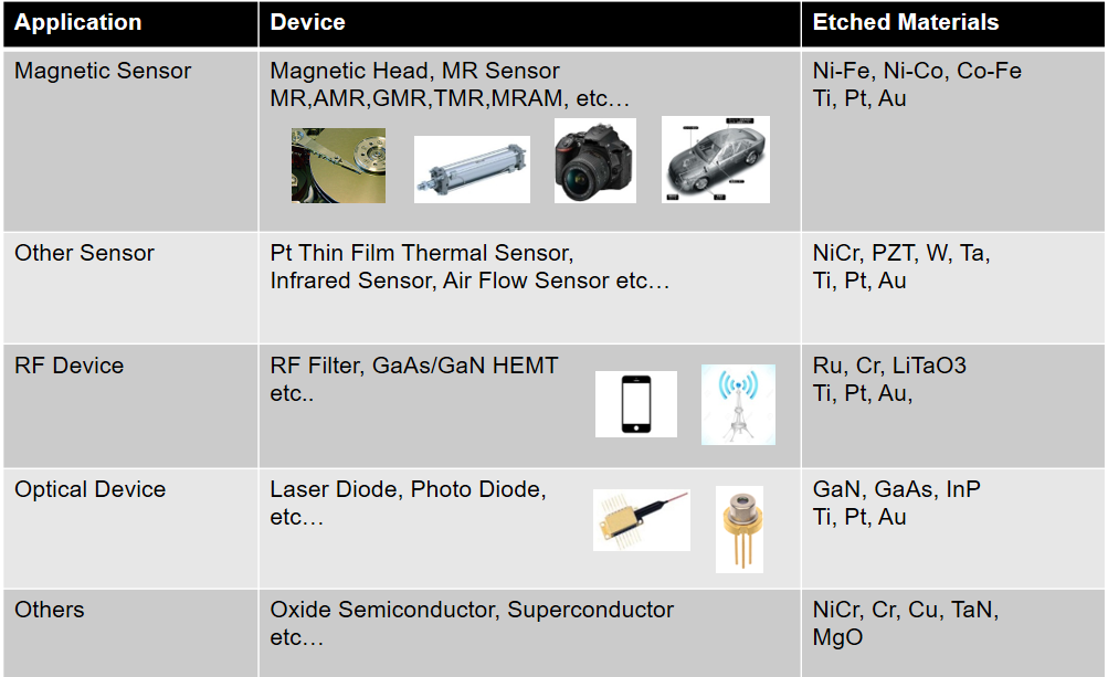
Ion Beam Etching (IBE) system is optimal etching technology for difficult-to etch materials such as Magnetic Materials, Gold, Platinum, Alloyed metals, and Compound semiconductor materials. IBE can be applied for materials which Reactive Ion Etching (RIE) cannot etch well.
IBE generates broad ion beam which strikes the substrate or wafer resulting in the removal of target materials.
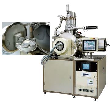
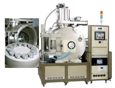
Planetary movement of stage and wafer holder called “Dry Chuck Planet” achieve excellent etching uniformity. It also features manual/motorized ion beam incident angle adjustment.
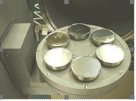
φ4” Dry Chuck Planet holders on Planetary Stage
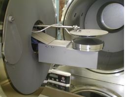
Stage Shutter for single stage
Shutter with a probe
to monitor ion current density
(Option)
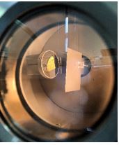
Tilting stage with motor drive
Direct Cooling/Indirect Cooling Stage /Gas Cooling Stage
Direct cooling circulates cooling water inside wafer holder for excellent cooling performance.
Indirect cooling stage enables Dry Chuck Planet removable. It reduces the downtime caused by setting wafers on the wafer holders (Dry Chuck Planet) with Dry Chuck Fixture.
In addition, Backside Gas cooling stage is available.
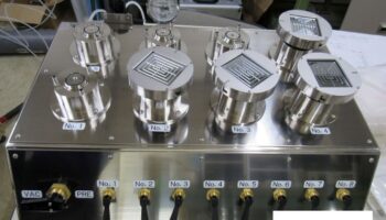
Dry Chuck Fixture for wafer exchange
Flexibility
We response to customer’s specific requirement as much as possible in designing of system and offer
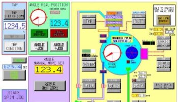
User friendly Touch panel screen interface
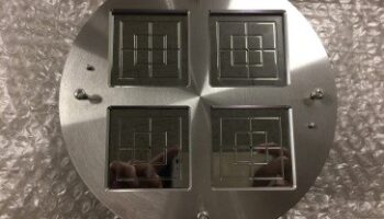
Customized Dry chuck planet holder
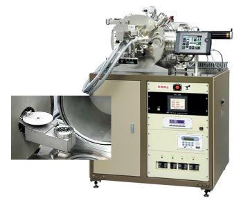
Specifications
Ion Source (GRID) Size: φ4cm, φ7.5cm, φ10cm
Stage: φ4″ Single Stage / Direct Cooling
Wafer Size: Up to φ4″
Etch Rate (nm/min) @ Si: > 10nm/min @ φ4cm IS
> 20nm/min @ φ7.5cm~ IS
Etch Uniformity (%): < ±6% @ φ60mm area @ φ4cm IS
< ±6% @ φ90mm area @ φ7.5cm~ IS
Wafer Temp (degree): < 100℃
Stage Angle: Manual
Specifications
Ion Source (GRID) Size: φ20cm
Stage : Pranetary (Rotation & Revolution)Stage
Direct/Indirect Cooling, Gas Cooling
Wafer Size: Up to φ8″
φ3″ x 8 wfs, φ4″ x 6 wfs, φ8″ x 1wf
Etch Rate (nm/min) @ Si: > 20nm/min
Etch Uniformity (%): < ±6% @ φ90mm area
Wafer Temp (degree): < 100℃
Stage Angle: Auto (Motor Drive)
Application
Ion Source (GRID) Size: φ20cm
Stage: Pranetary (Rotation & Revolution)Stage
Direct/Indirect Cooling
Wafer Size: φ4″ x 12 wfs, φ5″ x 10wfr, φ6″ x 8 wfr
*option: large substrate
Etch Rate (nm/min) @ Si: > 20nm/min
Etch Uniformity (%): < ±6% @ φ90mm area
Wafer Temp (degree): < 100℃
Stage Angle: Auto (Motor Drive)
Cross sectional TEM image of
Multi Tunnel Junction (MTJ) etching profile
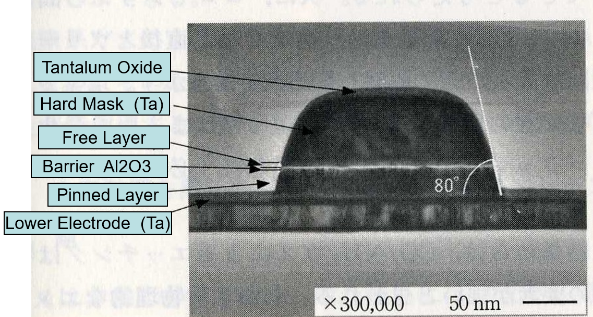
Cross sectional TEM image of
Multi Tunnel Junction (MTJ) etching profile
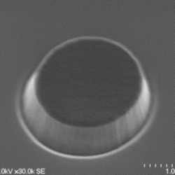
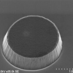
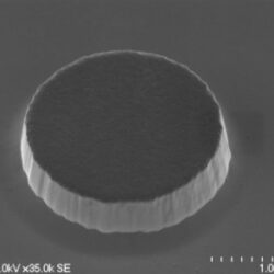
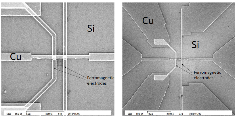
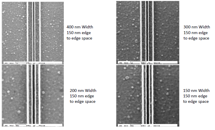
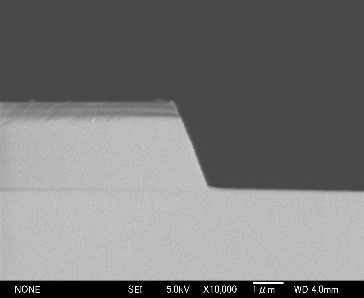
SEM images of ferromagnetic electrode by the ion beam etching